Back to: Build a 6502 based computer
To achieve the memory map that I have planned, I need some address decoder logic. This role here is to make sure that the correct ICs are using the address bus at the correct time. I will use 74 series logic chips to accomplish this.
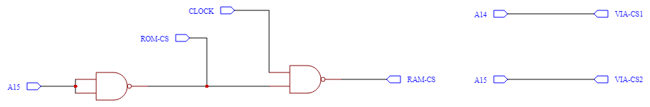
The RAM (62256), ROM (28256) and VIA (6522) have chip select pins. These pins need to be activated at the right point, this will be achieved with the address decoder logic.
Figure 1 shows my design for the address decoder logic. The circuit requires NAND and NOT gates. I could use the 7400 for NAND gates and the 7404 for NOT gates or I could use the 4011 for NAND gates and the 4009 for NOT gates. Both of these series of logic ICs are of the correct era but I am going with the 74 series.

This can be improved to bring the chip count down by one, by using one of the unused NAND gates to make a NOT gate, see figure 2.
The two main families are the 74 and 4000 series. I have chosen to use the 74 series. The two families have various positives and negatives but the main one that I am interested in here is propagation delay. Propagation delay is the length of time taken for a signal at a gate’s input to have an effect on the output of a gate. There are many circuits where this propagation delay would not be a problem. However, high-speed digital circuits are not one of them! The 4000 series are slower than the 74 series. Even though I have settled for the 74 series as my choice for logic chips. there is a further consideration to make, which family? There are TTL, CMOS and BI-CMOS versions, which can then be further broken down into TTL (74, 74L, 74H, 74S, 74LS, 74AS, 74ALS, 74F), CMOS (74C, 74HC, 74HCT, 74AC, 74ACT, 74ACQ, 74AHC, 74ALVC, 74ALVT, 74AUC, 74AUP, 74AVC, 74AXC, 74FC, 74FCT, 74LCX, 74LV, 74LVC, 74LV-A, 74LVT, 74LVQ, 74LVX, 74VHC) and BI-CMOS (74BCT and 74ABT).
I chose CMOS as they contain a few possibilities but my choice was the HC series. The propagation delays are lower than most of the other choices. The 4000 series is often slower than the 74 series. The HC series is an improvement from its predecessors. The improvements that we are interested in are the input and output rise and fall times. There are others, that in theory would be an even better choice but are harder to obtain! Of the CMOS 74 series the HC and HCT are two variants that are commonly used. The HCTs are good but for this project I chose HC. The reason for this is that there are a number of ICs that I’m using that are CMOS (65C02, 65C22, 28C256) and the HC variant will be ‘more compatible.’
It is good practice to keep to one family for your ICs, then there is less chance of problems, such as logic levels. Often mixing families works but you could run into problems that are hard to isolate. Often I have made circuits with a mix of families and everything has worked but when I make the final product I always use one family to ensure no compatibility problems.
At low clock speeds the propagation delay will probably not be an issue. However, with increases in clock speed, eventually, the propagation delay would likely be a limiting factor to how fast a clock speed I could use for the computer.
Between the a15 from the CPU, the chip select of the ROM needs to be inverted. Therefore I will need a NOT gate. The chip select of the RAM needs to be at logic 0 (since it is active low) when the clock signal is low and a15 from the CPU is 0. A NAND gate fulfils this requirement.