Back to: Build a 6502 based computer
I now have a 6502 that is reading the OpCode NOP (EA), causing the program counter to increment the address on the address bus by one, for every two clock cycles. This is effectively a hard-wired program! This is a good proof of concept but what I now want to be able to do is to be able to write programs. To do this I will need somewhere to store those programs.
In ROM is where I would like to store these programs. ROM (Read Only Memory) is a form of permanent storage. A program can be placed in ROM and will remain there, even if power is removed. There are many types of ROM but the type that I am interested in using here is EEPROM (Electrically Erasable Programmable Read Only Memory). EEPROMs can be reprogrammed by applying specific voltages to them.
With a program in the ROM, its contents are accessed by the 6502, by looking at different addresses on an address bus and reading what’s on a data bus.
The EEPROM that I will be using is a 28256. The 256 means that it can store 256Kb, or 32KB (256,000 / 8).
There are also 3 control pins: CE, WE, and OE.
CE
CE is the Chip enable pin. When this pin is LOW, read and write operations can occur. Bringing the pin HIGH inhibits all read and write operations.
WE
Write enable
OE
Output enable
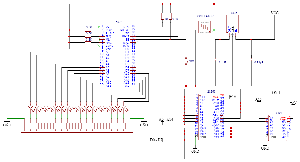
Like the 6502, the 28256 has a data and address bus. This means that they can be made to talk to each other, by connecting them together. However, there is a difference in the size of the address buses! The 6502 has a 16-bit address bus and the 28256 has a 15-bit address bus! This means that the 6502 can see from 0000000000000000 – 1111111111111111, which is FFFF in hex and the 28256 can see from 000000000000000 – 111111111111111, which is 7FFF in hex. Therefore, if the 6502 tries to access addresses on the 28256 higher than 7FFF, it won’t work!
This causes a problem because there will be one pin of the address bus of the 6502 that can not be connected to the address bus of the 28256 and therefore a range of addresses that the 28256 will not be able to read! The way that I will solve this is to use the fact that the most significant bit (A15) of the 6502 will be high when at the addresses that the 28256 cannot reach. If I connect A15 from the 6502 to the chip select pin on the 28256 (which is active low), when A15 is high, the 28256 will be off!
This solves one problem but creates another! When the 6502 is turned on and has been through its startup sequence, it looks at locations FFFC and FFFD for a program to execute. Any program that I have on the ROM would not be read, since the ROM cannot see anything in that range. One solution is to invert the bit from the A15 connection from the 6502 to the chip select on the 28256. This then alters the addresses that the 28256 can see to the range of 8000 – FFFF.
I can use an inverter to reverse the bit coming from the A15 of the 6502. I have removed the 8 resistors that I used to make the 6502 read NOPs. The circuit now looks like this:
Previously I mentioned that the 6502 that I’m using can work up to 14MHz (and maybe higher) but factors (such as other components) can limit the theoretical speed. The ROM is one of these components! Looking at the datasheet I can see that the read access time is 150ns. This means that the clock speed cannot be faster than 7MHz. If you were thinking that 150ns works out to close to 14MHz, this is not the case with a 6502! This is because the 6502 accesses memory on half of a clock cycle! In theory, I would need a ROM with at least a 70ns read access time. However, it would be interesting to see how much the ROM speed can be pushed. As well as trying to overclock the 6502, another fun addition would be to try and overclock the 28256.
My computer now has additional memory, in the form of ROM, to store programs that I write. It would be good to test that everything is working by writing a program. A good program would be to replicate the NOP in software, instead of hardware. If everything is working correctly, then I should see the same outcome as before – the address is incremented by one, every two clock cycles.
To program the ROM I need a programmer. These can be purchased or you could do as I have, I have made one! If you’re interested in making your own and/or you would like to learn about the hardware and software required, I have a course that I have written for this: build an EEPROM programmer
rom = bytearray([0xea] * 32768)Software Data Protection
The 28C256 comes with software data protection built into it. This can be enabled or disabled. When enabled, any attempts to write to it will not be successful.
To enable software data protection, the follows steps need to be taken:
- load data AA to address 5555
- load data 55 to address 2AAA
- load data A0 to address 5555
- load data XX to any address
- load last byte to last address
To disable software data protection, the follows steps need to be taken:
- load data AA to address 5555
- load data 55 to address 2AAA
- load data 80 to address 5555
- load data AA to address 5555
- load data 55 to address 2AAA
- load data 20 to address 5555
- load data XX to any address
- load last byte to last address